Soft4Sense
Smart Surfaces for Reliable Tooling Integration
Desafio
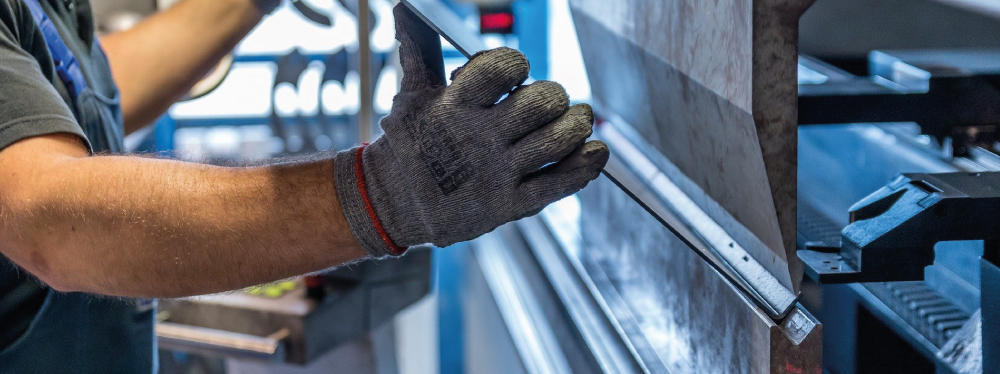
Utilização da tecnologia de filmes finos por pulverização catódica para miniaturização de sensores, para aplicação direta em componentes mecânicos submetidos a esforços, e avaliação dos parâmetros dos materiais na localização exata. Otimização do processo de forma a melhorar a integridade mecânica e elétrica desses dispositivos, para permitir a reprodutibilidade e fiabilidade na sua utilização.
Solução / Objetivo Principal
O objetivo é tornar disponível um software capaz de fornecer as informações necessárias para depositar o revestimento fino, sem problemas de integridade mecânica e elétrica. A solução proposta é um software que pode ajudar a depositar as multicamadas com as condições adequadas para a realização de um produto confiável e reprodutível. Este programa, a partir das informações sobre as características exigidas das camadas (por exemplo, nível de tensão residual, densidade de defeitos, características elétricas, dureza, módulo de Young´s), fornece as condições de deposição para o fabrico de multicamadas.
Objetivos, Atividades e Resultados esperados / atingidos
Objetivos Finais:
1. Desenvolvimento e otimização de novos materiais em filme finos a serem integrados num sistema multicamada com propriedades sensíveis. Compreender o nível de contaminação nas interfaces e seu efeito na delaminação do sistema completo.
2. Desenvolvimento de um modelo para prever a fiabilidade termomecânica do sistema multicamada, considerando as propriedades dos materiais e aplicação alvo. Correlação entre a informação extraída do modelo e o nível de tensões residuais. Ajuste das condições de deposição aos parâmetros do modelo.
3. Análise experimental das propriedades termo resistivas da camada funcional e consequências da integração em abordagem multicamada.
Seleção de uma aplicação para testar o sistema multicamadas em serviço.
Resultados Finais:
1. Sistema multicamada depositado em substratos de serviço com integridade mecânica para suportar a carga externa, com características elétricas adequadas para avaliação de temperatura.
2. Metodologia para preparação de superfícies e interfaces, e conhecimento estrutural e químico completo das interfaces entre as camadas do sistema.
3. Cálculo das tensões normais e de corte em multicamada e camada única, e modelo autónomo para previsão do módulo de elasticidade e do limite elástico.
4. Medição de temperatura de corte em tempo real e transmissão de dados em operações de maquinagem.

Referência do projeto
POCI-01-0247-FEDER-045921Financiamento
Região de Intervenção
Norte (32,08%) e Centro (67,92%)Investimento Total
971.167,64Investimento do IPN
304.676,22Elegível Total
971.167,64Elegível do IPN
304.676,22Apoio Financeiro da UE - Total
727.142,94Apoio Financeiro da UE – IPN
228.507,17Apoio Financeiro Público Nacional – Total
244.024,70Apoio Financeiro Público Nacional – IPN
76.169,05Duração
39 MesesData de Início
1 de Abril de 2020Data de Fim
30 de Junho de 2023Data de Aprovação
14 de Fevereiro de 2020Consórcio
TEandM – Tecnologia, Engenharia e Materiais S.A.Instituto Pedro Nunes
International Iberian Nanotechnology Laboratory
Parceiros
University of Texas at AustinPalavras-chave
Software de simulação;Filmes finos multicamada;
Pulverização catódica;
Superfícies funcionais.


